


Lattice Semiconductor Nexus Platform

Lattice Semiconductor Nexus Platform combines Lattice's long-standing low-power FPGA expertise with leading 28nm fully depleted silicon-on-insulator (FD-SOI) semiconductor manufacturing technology. With this platform, Lattice enables the rapid development of multiple device families that deliver low power, high performance, high reliability, and a small form factor.
Three levels of innovation are provided by the Lattice Nexus FPGA Platform:
- Circuit: 75% lower power, 100x lower soft error rate as compared with the bulk process
- Architecture: Embedded large RAM blocks optimize the implementation of common AI algorithms
- Solutions: Delivering more complete solutions with IP, reference designs, and software stacks
Videos
Circuit

- Programmable back bias enabled by the insulated gate of FD-SOI technology delivers performance/power optimization
- Critical area (orange) size reduction provides 100x SER reliability improvement
- FD-SOI leverages bulk CMOS process and has fewer processing steps
Architecture

- Optimized for Edge computing with embedded large RAM
- Improves performance by avoiding off-chip memory access
- Eliminates power consumption associated with accessing external memory
Solutions

- Solutions focus on AI, embedded vision, and security
- Reference design, kits, soft IP, and software accelerate product development
- Complete end-to-end solution offerings enable faster time-to-market
Development Tools
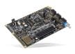
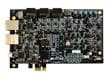
Lattice Semiconductor CrossLink-NX™ Evaluation Board
Demonstration and prototyping platform based on the CrossLink-NX Field Programmable Gate Array.
Lattice Semiconductor CrossLink-NX™ VIP Sensor Input Board
Enables designers to experiment with the embedded vision features of the CrossLink-NX FPGA.
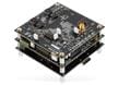
Lattice Semiconductor CrossLink-NX Voice & Vision Machine Learning Board
Designed for low power machine learning applications using CrossLink-NX 40K, a powerful FPGA.
Lattice Semiconductor Embedded Vision Development Kit
Modular development platform designed to enable a variety of embedded vision applications.
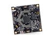
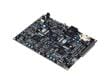
Lattice Semiconductor Certus-NX Versa Development Board
Connectivity platform featuring 5G PCIe and SGMII.
Lattice Semiconductor Sentry Demo Board
A 384-bit cryptography demonstration and test platform on a single board.
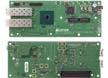
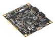
Lattice Semiconductor CertusPro™-NX Sensor to Ethernet Bridge Board
Features the CertusPro-NX-100 FPGA & CrossLink-NX-17, which output to a host system over Ethernet.
Related Platforms
Lattice Semiconductor Nexus™ 2 FPGA Platform
Advances power and performance efficiency, connectivity, and security compared to similar products.
Lattice Semiconductor Avant Platform
Powers top-tier, low-power, mid-range FPGA families.
Related FPGAs
Lattice Semiconductor CertusPro™-NX General-Purpose Low-Power FPGAs
Features up to eight SERDES lanes supporting up to 10.3Gbps per lane and ranges from 9mm2 to 27mm2.
Lattice Semiconductor Certus™-NX FPGAs
Supplies up to twice the I/O density per mm2 compared to similar competing FPGAs.
Lattice Semiconductor CrossLink-NX™ FPGAs
Built on the 28nm FD-SOI Lattice Nexus platform.
Lattice Semiconductor Mach-NX FPGAs
Delivers heightened security features and fast, power-efficient processing for HRoT implementation.

Lattice Semiconductor MachXO5™-NX Advanced Secure Control FPGAs
Features embedded flash, high I/O, and best-in-class security.
Lattice Semiconductor Avant Platform
Powers top-tier, low-power, mid-range FPGA families.