


Microchip Technology PIC16(L)F18426/46 Low Pin Count MCUs
Microchip PIC16(L)F18426/46 Low Pin Count MCUs combine eXtreme Low-Power (XLP) with Core Independent Peripherals (CIPs), Intelligent Analog, and communication peripherals for various applications. These MCUs feature a 12-bit Analog-to-Digital Converter with Computation (ADC2), Device Information Area (DIA), Memory Access Partitioning (MAP), and Peripheral Pin Select (PPS). The PIC16(L)F18426/46 low pin count MCUs have up to 28kb program flash memory, 2kb data SRAM memory, and 256B data EEPROM memory. These MCUs have various digital peripherals, including four Configurable Logic Cells (CLCs), two Complementary Waveform Generators (CWGs), and 18 I/O pins. The analog peripherals include ADC, DAC, Zero-Cross Detect (ZCD), temperature sensor circuit, and Fixed Voltage Reference (FVR) module. The PIC16(L)F18426/46 low pin count MCUs employ power-saving operation modes wherein the CPU, and the peripherals run at different cycle rates. These low pin count MCUs are ideal for a wide range of general-purpose and low-power applications.
Features
- C compiler optimized RISC architecture
- Operating speed
- 32MHz clock input for DC
- 125ns minimum instruction cycle
- Interrupt capability
- 16-level deep hardware stack
- Timers
- Up to two 24-bit timers
- Up to four 8-bit timers
- Up to four 16-bit timers
- Windowed Watchdog Timer (WWDT)
- Variable prescaler selection
- Variable window size selection
- Configurable in hardware and/or software
- Low-current Power-on Reset (POR)
- Configurable Power-up Timer (PWRT)
- Brown-out Reset (BOR)
- Low-Power BOR (LPBOR) option
- Memory
- Up to 28kb program flash memory
- Up to 2kb data SRAM memory
- 256 bytes data EEPROM
- Programmable code protection
- Direct, indirect, and relative addressing modes
- Memory Access Partition (MAP)
- Write-protect
- Customizable partition
- Operating voltage range
- 1.8V to 3.6V (PIC16LF184XX)
- 2.3V to 5.5V (PIC16F184XX)
- Operating temperature range
- -40ºC to 85ºC for industrial operation
- -40ºC to 125ºC for extended operation
- Power-saving operation modes
- Doze - CPU and peripherals run at different cycle rates
- Idle - CPU halted while peripherals operate
- Sleep - Lowest power consumption
- Extreme Low-power mode (XLP)
- Peripheral Module Disable (PMD) - Ability to selectively disable hardware module to minimize active power consumption of unused peripherals
- eXtreme Low-Power (XLP) features
- Sleep mode - 50nA @ 1.8V
- Watchdog timer - 500nA @ 1.8V
- Secondary Oscillator - 500nA @ 32kHz
- Operating current
- 8µA @ 32kHz, 1.8V
- 32µA/MHz @ 1.8V
- Digital peripherals
- Configurable Logic Cell (CLC)
- 4 CLCs
- Integrated combinational and sequential logic
- Complementary Waveform Generator (CWG)
- 2 CWGs
- Rising and falling edge dead-band control
- Full-bridge, half-bridge, and 1-channel drive
- Multiple signal sources
- Capture/Compare/PWM (CCP) modules
- 4 CCPs
- 16-bit resolution for Capture/Compare modes
- 10-bit resolution for PWM mode
- Pulse-Width Modulators (PWM)
- 2 10-bit PWMs
- Numerically Controlled Oscillator (NCO)
- 0Hz<fNCO
- fNCO/220 resolution
- Peripheral Pin Select (PPS)
- I/O pin remapping of digital peripherals
- Serial communications
- EUSART
- 1 EUSART (s)
- RS-232, RS-485, and LIN compatible
- Auto-baud detect and auto-wake-up on start
- Master Synchronous Serial Port (MSSP)
- 2 MSSP(s)
- SPI
- I2C, SMBus, and PMBus™ compatible
- EUSART
- Data Signal Modulator (DSM)
- Up to 18 I/O pins
- Timer modules
- Configurable Logic Cell (CLC)
- Analog peripherals
- Analog-to-Digital Converter with Computation (ADC2)
- Zero-Cross Detect (ZCD)
- Temperature sensor circuit
- Comparator
- Digital-to-Analog Converter (DAC)
- Fixed Voltage Reference (FVR) module
- Flexible oscillator structure
- High-precision internal oscillator
- 4x PLL for use with external sources
- 2x PLL for use with the HFINTOSC
- Low-Power Internal 31kHz Oscillator (LFINTOSC)
- External 32.768kHz Crystal Oscillator (SOCS)
Associated Products
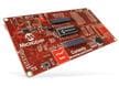
Microchip Technology Curiosity 8-bit Development Board
Full-featured development tool for Microchip 8-pin, 14-pin, and 20-pin 8-bit PIC® Microcontrollers.

Microchip Technology PIC16(L)F184x MCUs with XLP
Combine XLP technology with intelligent analog and different peripherals for various applications.
Microchip Technology PIC16(L)F18326/46 MCUs with XLP
Full-featured MCUs that feature analog, core independent peripherals, and communication peripherals.

Microchip Technology PIC16(L)F1847 Flash MCUs
Contains a mid-range CPU core with 49 instructions, 16 stack levels, and in-circuit debugging.

Microchip Technology PIC18 K42 Family Microcontrollers
Combines an array of CIPs, high-res analog, on-chip DMA, & vectored interrupts for fast processing.

Microchip Technology PIC16F18446 Curiosity Nano Kit (DM164144)
Compact development platform for the PIC16F18446 MCU, with full program and debug capabilities

Microchip Technology Curiosity Nano Base for Click Boards™ (AC164162)
Designed to ease the connection between Curiosity Nano Kits and Mikroe Click Boards™.
Additional Resources
Block Diagram
F18426/46 Low Pin Count MCUs")
Pin Diagram
F18426/46 Low Pin Count MCUs")
F18426/46 Low Pin Count MCUs")
F18426/46 Low Pin Count MCUs")
F18426/46 Low Pin Count MCUs")